
This year again, Jen-Hsun Huang’s keynote address was one, if not the moment of interest of the GPU Technology Conference. And yet, while NVIDIA CEO’s presentation unveiled a major update of the company’s technology roadmap, it also brought a number of questions. Of course, a roadmap is not a contractual commitment on the part of an industrial innovator. It is meant to give directions and a tenable technology vision over two to three years. It is along the way that the critical technical details are specified, especially those concerning implementation.
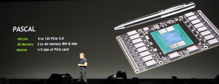
And so, we know now what to call the next NVIDIA GPU architecture. Introducing…”Pascal”, in honor of the inventor of the mechanical calculator, which came as a bit of a surprise. Within the community, some couldn’t help remark a bit of a delay based on the roadmap presented here last year. As we reported back then, Volta was supposed to be Maxwell’s successor. So what about it now? According to NVIDIA’s management, to whom we specifically asked, Volta remains scheduled, but at a later time. In that regard, the forthcoming Pascal is to be seen as a “refresh” of Maxwell. Don’t get confused…
That being said, it doesn’t really matter what the final name turns out to be. What does matter are the resulting technical specifications and features. And from this point of view, it’s the unified memory support that has now shifted to Pascal – or 2016. NVIDIA has officially confirmed that this much-awaited breakthrough will not be featured in Maxwell, whose notebook version (gm106) is already marketed and whose compute version (gm110) will probably come out early next year.
On the other hand, stacked memory, announced with Volta, will actually make it in Pascal. This DRAM memory, stacked directly upon the graphics processor, should at least double the bandwidth and thus substantially improve energy efficiency. According to Jen-Hsun Huang, the only limit to the space that can be added to the GPU is the price one is willing to pay. In fact, we should have about 2.5 times the current standard capacity, or about 30 GB.
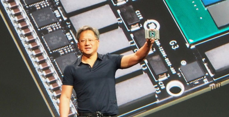
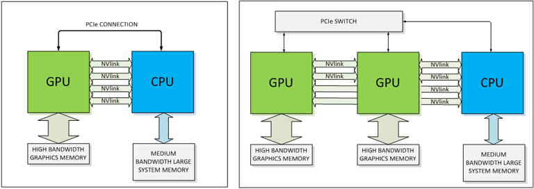
Beyond pure GPU architectures, the most “spectacular” innovation introduced this year is definitely NVLink, a point-to-point high-speed interconnect between GPU and CPU. This bus will not replace PCI Express but rather provide 5-12 times higher capacity bandwidth thanks to eight bi-directional lines of 20 Gb/s each. While the concept is quite promising in theory, what really matters here is how it will cooperate with Intel’s QPI given the chipmaker’s current market share in the server area. Would you be willing to bet on a trend inflexion in the next twenty-four months? In any case, that seems to be the strategy NVIDIA is pursuing. With last November’s announcement of a new collaboration with IBM to integrate Tesla accelerators in POWER servers, both parties may have a chance to establish a credible alternative to x86. For that matter, it goes without saying that POWER and NVLink have a lot to live up to.
Last, on the embedded and Tegra SoC front, the roadmap also evolves, which is not inconsistent with all of the above. The successor to Tegra K1 is no longer Parker, as announced (again) last year, but Erista. Scheduled for release in 2015, it will integrate a single 192-core Maxwell GPU with ARM cores – probably quad-core Cortex-A15s at first and then later on dual-core Denver 64-bit ARMv8. With 326 Gflops and a consumption of less than 10 Watts, these systems can rightfully claim the title of mini-supercomputers. They’re only missing the support of double precision arithmetic to figure among the most serious candidates in the race for exascale, all the more as they’re natively CUDA programmable.
More around this topic...


© HPC Today 2024 - All rights reserved.
Thank you for reading HPC Today.


