
With the fast development of image science and embedded system technique, it is widely accepted that future HPC systems will be limited by their power consumption. The current high performance computing system is a commodity server processors, design for many years to achieve maximum performance, and then it dawned on energy efficiency. In this paper we advocate a different approach: computer architecture based on distributed cluster structure. We introduce the architecture of Tibidabo, the first large-scale HPC cluster built from ARM multicore chips, and a detailed performance and energy efficiency evaluation. We now design experience and to improve the energy efficiency of future HPC systems based on the low power core. The experimental result shows the effectiveness of our methodology, further in-depth research portion is also discussed with case studies.
Introduction
In High Performance Computing (HPC), there is a continued need for higher computational performance. Science major challenges such as engineering, geophysics, bioinformatics, and other types of compute-intensive applications need a large amount of computing power. On the other hand, energy is becoming one of the most expensive resources, which greatly helps to run a large total cost of super computer facilities. In some cases, the total energy cost over a few years of operation can exceed the cost of the hardware infrastructure acquisition [1]. This trend is not limited to HPC systems, can also be applied to the data centers. Energy efficiency is already a primary concern for the design of any computer system and it is unanimously recognized that reaching the next milestone in supercomputers’ performance will be strongly constrained by power. The energy efficiency of a system will define the maximum achievable performance. In this article, we take the first steps in the solution by low power high performance computing system using the embedded and mobile devices. Use the CPU from the domain, however, is a challenge. Most embedded CPUs lack a vector floating-point unit and their software ecosystem is not tuned for HPC. What makes them particularly interesting is the size and power characteristics which allow for higher packaging density and lower cost. In the following three subsections we further motivate our proposal from several important aspects.
The Road to Exascale and ARM Processor
To illustrate our point about the need for low-power processors, let us reverse engineer a theoretical Exaflop supercomputer that has a power budget of 20 MW. An Exaflop machine will require 62.5 million of such cores, independently of how they are packaged together (multicore density, sockets per node). We also assume that only 30-40% of the total power will be actually spent on the cores, the rest going to power supply overhead, interconnect, storage, and memory. That leads to a power budget of 6 MW to 8 MW for 62.5 million cores, which is 0.10 W to 0.13 W per core. Current high performance processors integrating this type of cores require tens of watts at 2 GHz. However, ARM processors, designed for the embedded mobile market, consume less than 0.9 W at that frequency and thus are worth exploring even though they do not yet provide sufficient level of performance and they have a promising roadmap ahead. There is already a significant trend towards using ARM processors in data servers and cloud computing environments [2]. Those workloads are constrained by I/O and memory subsystems, not by CPU performance. Recently, ARM processors are also taking significant steps towards increased double-precision floating-point performance, making them competitive with state-of-the-art server performance. Previous generations of arm application processor has no function Floating-point unit can support HPC1 required throughput and delay. The ARM A9 architecture has an optional VFPv3 floating-point unit [2] and/or neon single instruction multiple data (SIMD) floating point unit [3]. VFPv3 unit is the assembly line, each cycle is able to perform a double add operation, or a MUL (fused multiply accumulation) every two cycles. The neon unit is the SIMD units support only integer and single precision point operand to the HPC itself less attractive. Then, use a double floating point arithmetic instructions per cycle (VFPv3), 1 GHz architecture provide 1-A9 GFLOPS peak. Recently arm architecture (A15 [4] processor has a completely pipelining double-precision floating-point unit and provide 2 GFLOPS 1 GHz per cycle (FMA). The new ARMv8 instruction set, which is being implemented in next-generation ARM cores, namely the Cortex-A50 Series [5], features a 64-bit address space, and adds double-precision to the NEON SIMD ISA, allowing for 4 operations per cycle per unit leading to 4 GFLOPS at 1 GHz.
Bell’s Law and Contribution
Our approach for an HPC system is novel because we argue for the use of mobile cores. We consider the improvements expected in mobile SoCs in the near future that would make them real candidates for HPC. As Bell’s states [6], a new computer class is usually based on lower cost components, which continue to evolve at a roughly constant price but with increasing performance from Moore’s law. This trend holds today: the class of computing systems on the rise today in HPC is those systems with large numbers of closely-coupled small cores (BlueGene/Q and Xeon Phi systems). From an architectural point of view, we suggest that the in this computing the size of the performance of the class and its growth potential and the evolution of the mobile market. In this paper, we present Tibidabo, an experimental HPC cluster that we built using NVIDIA Tegra2 chips, each featuring a performance-optimized dual-core ARM Cortex-A9 processor. We use the PCIe support in Tegra2 to connect a 1 GbE NIC, and build a tree interconnect with 48-port 1 GbE switches. We do not intend our first prototype to achieve energy efficiency competitive with today’s leaders. The purpose of this prototype is to be a proof of concept to demonstrate that building such energy-efficient clusters with mobile processors is possible, and to learn from the experience. On the software side, the goal is to deploy an HPC-ready software stack for ARM-based systems, and to serve as an early application development and tuning vehicle. The contributions of this paper are:
- Have design of the first HPC ARM-based cluster architecture, with a complete performance evaluation, energy efficiency evaluation, and comparison with state-of-the-art high-performance architectures.
- A power distribution estimation of our ARM cluster.
- Model-based performance and energy-efficiency projections of a theoretical HPC cluster with a higher multicore density and higher-performance ARM cores.
- Technology challenges and design guidelines based on our experience to make ARM-based clusters a competitive alternative for HPC.
The ARM Cluster Architecture Analysis
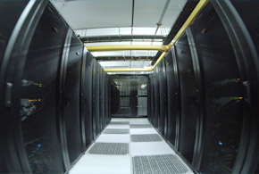
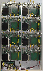
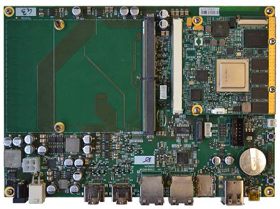
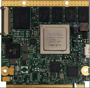
The computing chip in the Tibidabo cluster is the Nvidia Tegra2 SoC, with a dual-core ARM Cortex-A9 running at 1 GHz and implemented using TSMC’s 40nm LPG performance-optimized process. Tegra2 features a number of application-specific accelerators targeted at the mobile market, such as video and audio encoder/decoder, and image signal processor, but none of these can be used for general-purpose computation and only contribute as a SoC area overhead. The GPU in Tegra2 does not support general programming models such as CUDA or OpenCL, so it cannot be used for HPC computation either. However, more advanced GPUs actually support these programming models and a variety of HPC systems use them to accelerate certain kind of workloads. Tegra2 is the central part of the Q7 module [7] (See Figure 1(a)). The module also integrates 1 GB of DDR2-667 memory, 16 GB of eMMC storage, a 100 MbE NIC (connected to Tegra2 through USB) and exposes PCIe connectivity to the carrier board. Using Q7 modules allows an easy upgrade when next generation SoCs become available, and reduces the cost of replacement in case of failure. These boards are organized into blades, and each blade hosts 8 nodes and a shared Power Supply Unit (PSU). In total, Tibidabo has 128 nodes and it occupies 42 U standard rack spaces: 32 U for compute blades, 4 U for interconnect switches and 2 U for the file server. These are the basic structure of the proposed system. At the time of writing of this paper this was the only MPI distribution that worked reliably with the SLURM job-manager in our cluster. We use ATLAS 3.9.51 [8] as our linear algebra library. This library is chosen due to the lack of a hand-optimized algebra library for our platform and its ability to auto-tune to the underlying architecture. Applications that need an FFT library rely on FFTW v3.3.1 [9] for the same reasons.
Fig.1: Components of the Tibidabo System
More around this topic...
In the same section


© HPC Today 2024 - All rights reserved.
Thank you for reading HPC Today.


